US 12,236,239 B2
Systems and methods for data placement for in-memory-compute
Krishna T. Malladi, San Jose, CA (US); and Wenqin Huangfu, San Jose, CA (US)
Assigned to Samsung Electronics Co., Ltd., Yongin-si (KR)
Filed by Samsung Electronics Co., Ltd., Suwon-si (KR)
Filed on Sep. 14, 2023, as Appl. No. 18/368,515.
Application 18/368,515 is a continuation of application No. 17/548,220, filed on Dec. 10, 2021, granted, now 11,782,707.
Application 17/548,220 is a continuation of application No. 16/859,829, filed on Apr. 27, 2020, granted, now 11,226,816, issued on Jan. 18, 2022.
Claims priority of provisional application 62/975,577, filed on Feb. 12, 2020.
Prior Publication US 2024/0004646 A1, Jan. 4, 2024
This patent is subject to a terminal disclaimer.
Int. Cl. G06F 9/30 (2018.01); G06F 7/53 (2006.01); G06F 7/57 (2006.01)
CPC G06F 9/3001 (2013.01) [G06F 7/5318 (2013.01); G06F 7/57 (2013.01); G06F 9/30036 (2013.01); G06F 9/30098 (2013.01); G06F 9/3016 (2013.01)] 20 Claims
OG exemplary drawing
 
1. A memory module comprising:
a dynamic random access memory (DRAM) device comprising:
an array of DRAM rows; and
an in-memory compute (IMC) module; and
a memory controller configured to:
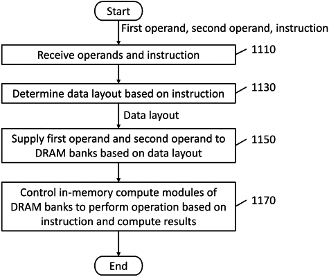
receive, from a host processor, an input data and an instruction; and
supply the input data to the DRAM device in a data arrangement selected based on the instruction, the data arrangement specifying placement of an operand among the array of DRAM rows and the IMC module,
wherein the IMC module is configured to perform an operation on the input data based on the instruction.