| CPC G06F 3/0659 (2013.01) [G06F 3/061 (2013.01); G06F 3/0679 (2013.01); G06F 12/10 (2013.01); G11C 16/0483 (2013.01); G11C 16/10 (2013.01); G11C 16/26 (2013.01); G06F 2212/657 (2013.01)] | 20 Claims |
|
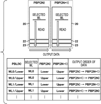
1. A semiconductor memory device comprising:
a first memory cell array that includes a plurality of first blocks, each first block including a plurality of first memory cells, each of the first memory cells capable of being set into one of n threshold voltage levels, n being an integer of 4 or more;
a plurality of first word lines, each first word line being connected to a gate of a corresponding one of the first memory cells in each of the first blocks;
a plurality of first bit lines electrically connected to one ends of the first memory cells of each first block, respectively;
a plurality of first sense amplifiers connected to the first bit lines, respectively;
a second memory cell array that includes a plurality of second blocks, each second block including a plurality of second memory cells, each of the second memory cells capable of being set into one of n threshold voltage levels;
a plurality of second word lines, each second word line being connected to a gate of a corresponding one of the second memory cells in each of the second blocks;
a plurality of second bit lines electrically connected to one ends of the second memory cells of each second block, respectively; and
a plurality of second sense amplifiers connected to the second bit lines, respectively, wherein
upon receipt of a first read command associated with a first address,
one of the first word lines is applied with i kinds of voltages, and one of the second word lines is applied with j kinds of voltages, i being an integer of 1 or more, j being an integer larger than i, and
upon receipt of a second read command associated with a second address,
the one of the second word lines is applied with k kinds of voltages, and the one of the first word lines is applied with 1 kinds of voltages, k being an integer of 1 or more, l being an integer larger than k.
|