US 12,236,115 B2
Flash memory controller
Tsung-Chieh Yang, Hsinchu (TW); Chun-Chieh Kuo, Taipei (TW); Ching-Hui Lin, Hsinchu County (TW); and Yang-Chih Shen, Taoyuan (TW)
Assigned to Silicon Motion, Inc., Hsinchu County (TW)
Filed by Silicon Motion, Inc., Hsinchu County (TW)
Filed on Jan. 15, 2024, as Appl. No. 18/412,635.
Application 18/412,635 is a continuation of application No. 17/324,121, filed on May 19, 2021, granted, now 11,914,873.
Application 17/324,121 is a continuation of application No. 17/030,392, filed on Sep. 24, 2020, granted, now 11,048,421, issued on Jun. 29, 2021.
Application 17/030,392 is a continuation of application No. 16/686,200, filed on Nov. 17, 2019, granted, now 10,824,354, issued on Nov. 3, 2020.
Application 16/686,200 is a continuation of application No. 16/260,142, filed on Jan. 29, 2019, granted, now 10,521,142, issued on Dec. 31, 2019.
Application 16/260,142 is a continuation of application No. 15/985,718, filed on May 22, 2018, granted, now 10,235,075, issued on Mar. 19, 2019.
Application 15/985,718 is a continuation of application No. 15/643,501, filed on Jul. 7, 2017, granted, now 10,007,460, issued on Jun. 26, 2018.
Application 15/643,501 is a continuation of application No. 15/235,128, filed on Aug. 12, 2016, granted, now 9,733,857, issued on Aug. 15, 2017.
Application 15/235,128 is a continuation of application No. 14/983,566, filed on Dec. 30, 2015, granted, now 9,588,709, issued on Mar. 7, 2017.
Application 14/983,566 is a continuation of application No. 14/596,236, filed on Jan. 14, 2015, granted, now 9,256,529, issued on Feb. 9, 2016.
Application 14/596,236 is a continuation of application No. 13/491,377, filed on Jun. 7, 2012, granted, now 9,075,709, issued on Jul. 7, 2015.
Claims priority of application No. 100129676 (TW), filed on Aug. 19, 2011.
Prior Publication US 2024/0152288 A1, May 9, 2024
This patent is subject to a terminal disclaimer.
Int. Cl. G11C 7/00 (2006.01); G06F 3/06 (2006.01); G06F 12/02 (2006.01); G11C 11/56 (2006.01)
CPC G06F 3/0634 (2013.01) [G06F 3/0604 (2013.01); G06F 3/064 (2013.01); G06F 3/0679 (2013.01); G06F 12/0246 (2013.01); G11C 11/5628 (2013.01); G11C 11/5642 (2013.01); G06F 2212/7201 (2013.01); G06F 2212/7206 (2013.01); Y02D 10/00 (2018.01)] 5 Claims
OG exemplary drawing
 
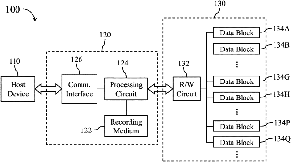
1. A method for accessing a flash memory module, wherein the flash memory module comprises a plurality of data blocks, and the method comprises the steps of:
receiving data from a host device;
determining if the data received from the host device is cold data or hot data;
if the data is determined as the cold data, using a two-bit-per-cell mode or a three-bit-per-cell mode to write the data into one of the plurality of data blocks; and
if the data is determined as the hot data, using a one-bit-per-cell mode to write the data into another one of the plurality of data blocks.