| CPC G06F 3/0616 (2013.01) [G06F 3/0631 (2013.01); G06F 3/0658 (2013.01); G06F 3/0673 (2013.01); G06F 12/0292 (2013.01); G06F 2212/1036 (2013.01)] | 20 Claims |
|
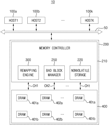
1. A memory system comprising:
a memory module including a plurality of semiconductor memory devices; and
a memory controller connected to at least one host through a serial interface, the memory controller configured to control the plurality of semiconductor memory devices, wherein
each of the plurality of semiconductor memory devices includes a memory cell array that includes a normal cell region and a redundancy region, and
each of the plurality of semiconductor memory devices is configured to provide the memory controller with an address of at least a first defective memory cell row from among defective memory cell rows in the normal cell region as an unrepairable address information, the at least first defective memory cell row being unrepairable with a redundancy resource of the redundancy region,
wherein the memory controller is configured to:
allocate a portion of the normal cell regions of at least one of the plurality of semiconductor memory devices as a reserved region;
remap a first unrepairable address to a first physical address of the reserved region in response to a first host physical address from the at least one host matching the first unrepairable address in the unrepairable address information; and
remap a second unrepairable address to a second physical address of the reserved region in response to a second host physical address from the at least one host matching the second unrepairable address in the unrepairable address information, and
wherein the first physical address and the second physical address are consecutive.
|