| CPC G06F 3/0446 (2019.05) [G06F 3/0412 (2013.01); G06F 3/0443 (2019.05); G06F 2203/04107 (2013.01); G06F 2203/04111 (2013.01); H10K 59/40 (2023.02)] | 30 Claims |
|
1. An electronic device comprising:
a substrate;
a circuit layer on the substrate, and comprising a transistor;
a light emitting element layer on the circuit layer, and comprising a light-emitting element electrically connected to the transistor; and
a sensor layer on the light emitting element layer, and comprising:
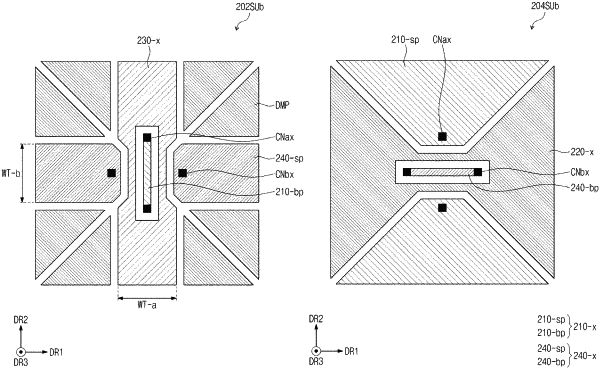
a first sensing electrode comprising first patterns, and a first bridge pattern electrically connected to the first patterns;
a second sensing electrode extending in a first direction and crossing the first sensing electrode;
a first electrode extending in a second direction crossing the first direction; and
a second electrode comprising second patterns, and a second bridge pattern electrically connected to the second patterns,
wherein:
one of the first patterns comprises a first region overlapping with the first electrode;
one of the second patterns comprises a second region overlapping with the second sensing electrode; and
a first area of the first region is less than a second area of the second region.
|