| CPC G06F 3/0412 (2013.01) [H10K 50/858 (2023.02); H10K 59/40 (2023.02); G06F 2203/04103 (2013.01); H10K 59/12 (2023.02)] | 26 Claims |
|
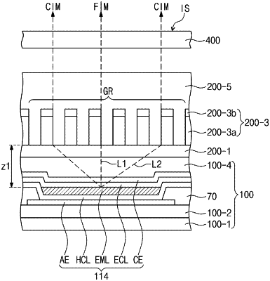
1. A display device comprising:
a display panel with a light emitting area from which a light exits is defined; and
an input sensor disposed on the display panel, the input sensor comprising:
a first conductive layer;
a first insulating layer disposed on the first conductive layer and provided with a diffraction grating defined therein to correspond to the light emitting area; and
a second conductive layer disposed on the first insulating layer and connected to the first conductive layer, the first insulating layer comprising:
a first sub-insulating layer covering the first conductive layer; and
a second sub-insulating layer disposed on the first sub-insulating layer, wherein the first sub-insulating layer and the second sub-insulating layer comprise a plurality of holes,
wherein the plurality of holes comprise sub holes to expose a portion of the first conductive layer and main holes defined in the first and second sub-insulating layers define the diffraction grating.
|