US 12,235,720 B2
Adaptive error correction to improve system memory reliability, availability, and serviceability (RAS)
Rajat Agarwal, Portland, OR (US); Hsing-Min Chen, Santa Clara, CA (US); Wei P. Chen, Portland, OR (US); Wei Wu, Portland, OR (US); Jing Ling, Milpitas, CA (US); Kuljit S. Bains, Olympia, WA (US); Kjersten E. Criss, Portland, OR (US); Deep K. Buch, Folsom, CA (US); Theodros Yigzaw, Sherwood, OR (US); John G. Holm, Beaverton, OR (US); Andrew M. Rudoff, Boulder, CO (US); Vaibhav Singh, Hillsboro, OR (US); and Sreenivas Mandava, Los Altos, CA (US)
Assigned to Intel Corporation, Santa Clara, CA (US)
Appl. No. 18/268,956
Filed by Intel Corporation, Santa Clara, CA (US)
PCT Filed Dec. 26, 2020, PCT No. PCT/US2020/067075
§ 371(c)(1), (2) Date Jun. 21, 2023,
PCT Pub. No. WO2022/139849, PCT Pub. Date Jun. 30, 2022.
Prior Publication US 2024/0061741 A1, Feb. 22, 2024
Int. Cl. G06F 11/10 (2006.01)
CPC G06F 11/10 (2013.01) 20 Claims
OG exemplary drawing
 
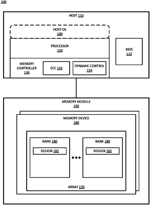
1. A memory device comprising:
a memory array with N banks, addressable by a memory controller for active access;
error checking and correction (ECC) logic to detect a bank failure of one of the N banks (“failed bank”); and
control logic to copy contents of the failed bank to distribute to the other (N-1) banks in a designated region of each of the other (N-1) banks and indicate reduction of memory space available for active access from N banks to the other (N-1) banks to the memory controller.