| CPC G06F 1/185 (2013.01) [G06F 1/186 (2013.01); H01R 12/72 (2013.01); H05K 1/117 (2013.01); H05K 7/1417 (2013.01); H01L 23/5386 (2013.01); H05K 1/181 (2013.01)] | 17 Claims |
|
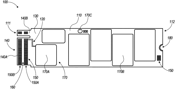
1. An electronic device, comprising:
a substrate having a substrate body;
a first interconnect region proximate a first end of the substrate, the first interconnect region includes:
a first set of interconnects; and
a second set of interconnects physically separated from the first set of interconnects by an inactive region, wherein:
the first set of interconnects are located between the inactive region and the substrate body;
the second set of interconnects are located between the inactive region and a perimeter edge of the first interconnect region; and
the first set of interconnects and the second set of interconnects are configured for electrical communication between a socket and
one or more die coupled with the substrate; and
one or more electrical traces in communication with the second set of interconnects, wherein the one or more electrical traces are located at least partially within a footprint of the first set of interconnects.
|