| CPC G06F 1/1656 (2013.01) [G06F 1/1643 (2013.01); G06F 3/0442 (2019.05); H05K 1/181 (2013.01); H05K 9/0075 (2013.01); H05K 9/0088 (2013.01); H05K 2201/10128 (2013.01)] | 14 Claims |
|
1. An electronic device comprising:
a display panel;
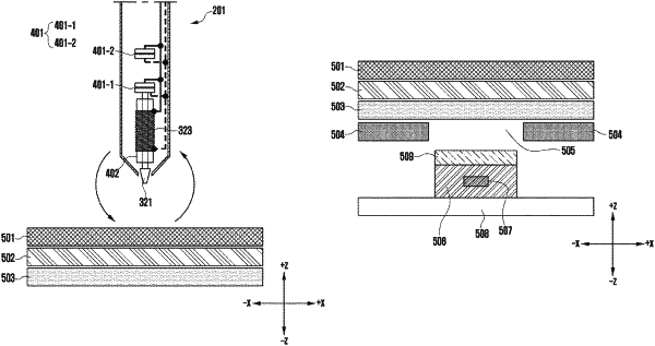
a recognition member disposed under the display panel and including a conductive pattern to recognize a signal from a pen input device;
a first shielding member disposed under the recognition member and including a soft magnetic material to shield a magnetic field generated from the pen input device;
a second shielding member disposed under the first shielding member and including a conductive material to shield electromagnetic waves generated from an electronic component; and
a third shielding member disposed under the second shielding member, covering electronic components from a bottom of the second shielding member, and including a soft magnetic material to shield magnetic fields generated from the electronic components,
wherein the second shielding member includes a component region corresponding to the electronic component, wherein the electronic component is disposed under the second shielding member, and at least one hole formed in the component region; and
wherein the hole corresponds to a magnetic material disposed inside the electronic component.
|