| CPC G03F 7/0002 (2013.01) [B82Y 30/00 (2013.01); B82Y 40/00 (2013.01)] | 17 Claims |
|
1. A method of manufacturing nano-structures on a substrate, the method comprising:
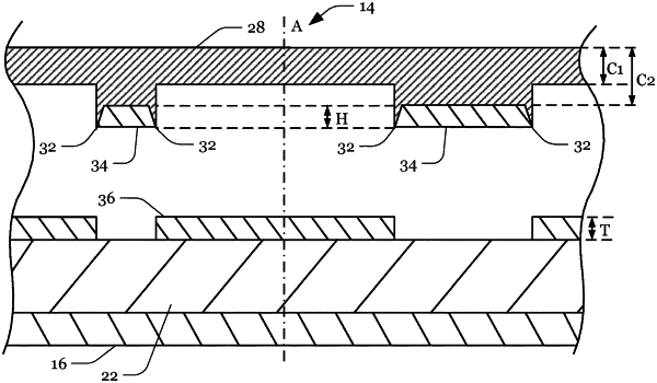
depositing a material layer on the substrate, wherein the material layer has a thickness below 1 μm;
moving a cutting die toward the material layer having the thickness below 1 μm, the cutting die having protruding portions each with a circumferential cutting edge that encircles an opening or a recess, the cutting edge of each protruding portion having a transverse cross section that is asymmetrical and that includes an inner side facing the opening or recess and an opposing outer side, the inner side comprising a barb or being sloped toward the opening or recess;
pressing the cutting die against the material layer so that the cutting edge of each protruding portion cuts out a portion of the material layer that is encircled by the cutting edge; and
removing the cut-out portions from the substrate.
|