|
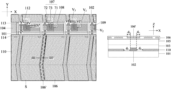
1. A display substrate, comprising: a base substrate; a plurality of data lines on the base substrate; a first insulating layer on a side of a layer where the plurality of data lines are positioned away from the base substrate; a plurality of gate lines a side of the first insulating layer away from the layer where the plurality of data lines are positioned, wherein an extension direction of each of the plurality of gate lines and an extension direction of each of the plurality of data lines are intersected; a second insulating layer on a side of a layer where the plurality of gate lines are positioned away from the first insulating layer; and a first electrode on a side of the second insulating layer away from the layer where the plurality of gate lines are positioned, wherein at least a portion of an orthographic projection of the first electrode on the base substrate is within an region surrounded by orthographic projections of two adjacent ones of the plurality of data lines on the base substrate and orthographic projections of two adjacent ones of the plurality of gate lines on the base substrate, wherein the display substrate further comprises: a transistor, wherein a gate of the transistor is in the same layer and made of the same material as the data line, a first electrode and a second electrode of the transistor are in the same layer and made of the same material as the gate line; the gate of the transistor is electrically connected to the gate line, and the first electrode of the transistor is electrically connected to the data line; and a first transfer electrode, which is in the same layer and made of the same material as the first electrode; wherein the first transfer electrode is electrically connected to the gate of the transistor through a first via penetrating through the first insulating layer and the second insulating layer, and is electrically connected to the gate line through a second via penetrating through the second insulating layer.
|
