| CPC G02F 1/136286 (2013.01) [G02F 1/134345 (2021.01); G02F 1/1368 (2013.01); H01L 27/124 (2013.01); G02F 2201/121 (2013.01); G02F 2201/123 (2013.01); G02F 2201/52 (2013.01)] | 20 Claims |
|
1. An array substrate, comprising:
a first base;
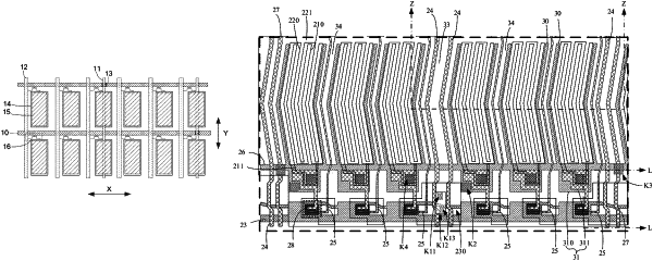
a plurality of pixel units arrayed on the first base in a row direction and a column direction; each of the pixel units comprising at least two sub-pixels arranged in the row direction;
a plurality of first scanning lines sequentially arranged on the first base in the column direction, at least one first scanning line being arranged at a side of each row of pixel units in the column direction, the first scanning lines being connected with the sub-pixels;
a plurality of second scanning lines sequentially arranged on the first base in the row direction, at least one second scanning line being arranged at a side of each column of pixel units in the row direction;
a plurality of data lines sequentially arranged on the first base in the row direction, the data line being connected with the sub-pixels, each of the data lines being arranged on at least one side of each column of sub-pixels in the row direction; and
a plurality of first common lines sequentially arranged on the first base in the column direction, the first common lines being connected with the sub-pixels, and at least one of the first common lines being arranged at the side of each row of pixel units in the column direction, wherein:
the second scanning line has a scanning signal input terminal and is connected with the first scanning line through a first via hole structure; and
each of the sub-pixels comprises:
a sub-pixel electrode having a plurality of first electrode strips arranged at intervals in the row direction;
a common electrode arranged in the same layer as the sub-pixel electrode, the common electrode having a plurality of second electrode strips arranged at intervals in the row direction, the second electrode strips and the first electrode strips being arranged alternately in the row direction, and the common electrode being connected with the first common line through a second via hole structure; and
a transistor comprising a gate, an active layer, a first electrode, and a second electrode arranged in the same layer, the gate being connected with the first scanning line, the first electrode being connected with an end of the active layer, the first electrode being connected with the data line, and the second electrode being connected with the other end of the active layer and connected with the sub-pixel electrode.
|