| CPC G02F 1/136227 (2013.01) [G02F 1/13439 (2013.01); H01L 27/1248 (2013.01); H01L 27/1288 (2013.01); G02F 1/134363 (2013.01); G02F 1/1368 (2013.01)] | 9 Claims |
|
1. An array substrate comprising:
a base substrate;
a thin film transistor disposed on the base substrate;
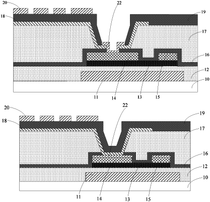
a first passivation layer, an organic film layer and a pixel electrode disposed on the thin film transistor;
a connection structure configured to connect a source electrode of the thin film transistor and the pixel electrode, wherein the connection structure is disposed in a via hole structure exposing the pixel electrode and the source electrode; and
a second passivation layer disposed on a side of the pixel electrode away from the base substrate;
wherein the connection structure is disposed in the via hole structure exposing the pixel electrode and the source electrode, and comprises: a first via hole exposing the source electrode formed on the first passivation layer, a second via hole communicated with the first via hole formed on the organic film layer, a third via hole communicated with the second via hole formed on the pixel electrode, a fourth via hole which communicates with the third via hole and exposes the pixel electrode formed on the second passivation layer, wherein the fourth via hole, the third via hole, the second via hole and the first via hole form the via hole structure exposing the pixel electrode and the source electrode, and the connection structure is connected to the pixel electrode through the via hole structure and is connected to the source electrode.
|