| CPC G02B 6/3546 (2013.01) [G02B 6/3508 (2013.01); G02B 6/12007 (2013.01); G02B 2006/12145 (2013.01); G02B 6/29344 (2013.01)] | 20 Claims |
|
1. A monolithically integrated photonics system on a substrate, the system comprising:
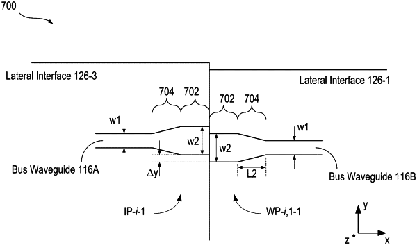
a first bus waveguide in a first region that is characterized by a first lithography reticle that is no larger than a maximum reticle size, the first bus waveguide having a first width and including a first coupling portion having a second width and a first taper region that optically couples the first bus waveguide and the first coupling portion;
a second bus waveguide in a second region that is characterized by a second lithography reticle that is no larger than the maximum reticle size, the second bus waveguide having the first width and including a second coupling portion having the second width and a second taper region that optically couples the second bus waveguide and the second coupling portion; and
a first coupling region that includes the first and second coupling portions;
wherein the first region abuts the second region such that the first and second bus waveguides are optically coupled via the first coupling region; and
wherein the system occupies an area that exceeds the maximum reticle size.
|