US 12,235,490 B2
Semiconductor structure and method for forming the same
Wei-Kang Liu, Taichung (TW); Lee-Shian Jeng, Hsinchu (TW); Chih-Tsung Shih, Hsinchu (TW); Hau-Yan Lu, Hsinchu (TW); and Yingkit Felix Tsui, Cupertino, CA (US)
Assigned to TAIWAN SEMICONDUCTOR MANUFACTURING COMPANY LTD., Hsinchu (TW)
Filed by TAIWAN SEMICONDUCTOR MANUFACTURING COMPANY LTD., Hsinchu (TW)
Filed on Jul. 1, 2022, as Appl. No. 17/810,578.
Prior Publication US 2024/0004131 A1, Jan. 4, 2024
Int. Cl. G02B 6/122 (2006.01); G02B 6/13 (2006.01)
CPC G02B 6/1228 (2013.01) [G02B 6/13 (2013.01)] 20 Claims
OG exemplary drawing
 
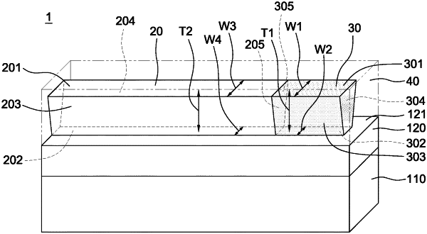
8. A semiconductor structure, comprising:
a waveguide disposed over a top surface of an oxide layer and configured to guide light; and
a doped structure connected to the waveguide, wherein the doped structure has a tapered shape that tapers in a direction normal to the top surface of the oxide layer, and the doped structure has a gradient dopant concentration decreasing in the direction.