| CPC G01S 7/4816 (2013.01) [H01L 27/1462 (2013.01); H01L 27/14627 (2013.01); H01L 27/14629 (2013.01); H01L 27/14636 (2013.01); H01L 27/14645 (2013.01); H01L 27/14649 (2013.01); G01S 17/894 (2020.01)] | 18 Claims |
|
1. A sensor chip, comprising:
a pixel array section comprising a plurality of pixels, wherein
the plurality of pixels includes:
a first set of pixels, and
a second set of pixels different from the first set of pixels, wherein the second set of pixels is outside a middle part of the pixel array section;
each pixel of the plurality of pixels includes:
a semiconductor substrate that includes:
a first surface;
a second surface, wherein the first surface is opposite to the second surface; and
an avalanche photodiode;
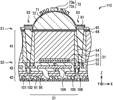
an on-chip lens on a side of the first surface of the semiconductor substrate;
a first reflective member that is on a front surface of the on-chip lens at a position which is opposite to the avalanche photodiode, wherein the position of the first reflective member on the on-chip lens is based on an image height of one of the first set of pixels or the second set of pixels in the pixel array section, wherein the first reflective member includes a main portion and a small portion separated from each other; and
a wiring layer on a side of the second surface of the semiconductor substrate, wherein the wiring layer includes a second reflective member.
|