| CPC G01R 19/175 (2013.01) [H02M 1/0009 (2021.05)] | 19 Claims |
|
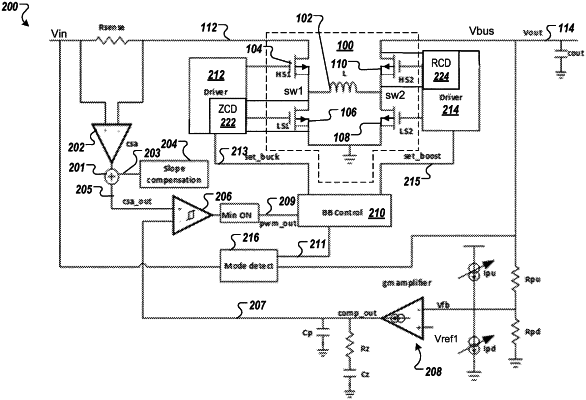
1. A Universal Serial Bus (USB) Type-C controller comprising:
a gate driver buck converter operable to couple to a first high-side switch and to a first low-side switch of a buck-boost converter, the buck-boost converter being capable of voltage swings of 20 volts or greater at an input and at an output of an inductor of the buck-boost converter;
a zero crossing detection (ZCD) comparator circuit, of the gate driver buck converter, coupled to the first low-side switch, wherein inputs of the ZCD comparator circuit comprise ground and the input of the inductor, and wherein the ZCD comparator circuit is to, while the buck-boost converter operates in buck mode:
detect a zero current flow through the first low-side switch; and
turn off the first low-side switch in response to detecting the zero current flow through the first low-side switch;
a gate driver boost converter coupled to a second high-side switch and to a second low- side switch of the buck-boost converter;
a reverse current detection (RCD) comparator circuit, of the gate driver boost converter, coupled to the second high-side switch, wherein inputs of the RCD comparator circuit comprise an output voltage and the output of the inductor, and wherein the RCD comparator circuit is to, while the buck-boost converter operates in boost mode:
detect a zero current flow through the second high-side switch; and
turn off the second high-side switch in response to detecting the zero current flow through the second high-side switch; and
control logic configured to enable programmable control of the ZCD comparator circuit and the RCD comparator circuit for one or more of:
a programming range in threshold reference voltages in each of the ZCD comparator circuit and the RCD comparator circuit; and
enabling and/or disabling of the ZCD comparator circuit or the RCD comparator circuit based on mode of operation.
|