| CPC G01R 1/071 (2013.01) [G02B 27/283 (2013.01); H01L 21/6833 (2013.01)] | 20 Claims |
|
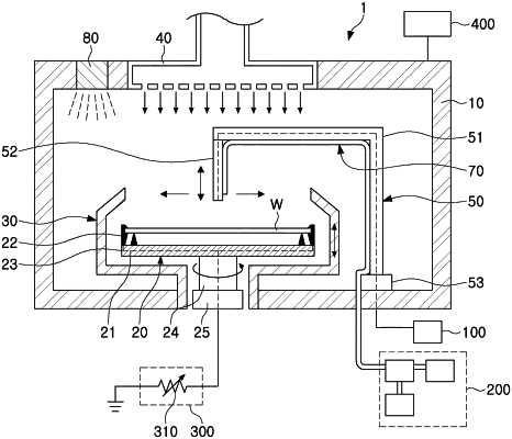
1. A substrate processing apparatus, comprising:
a chamber having an internal space configured for performance of a wet process therein;
a chuck in a lower region of the internal space;
a probe having one end above an upper portion of the chuck, and including an electro-optical crystal having an optical refractive index configured to change in proportion to a magnitude of an electric field applied at an upper portion of a semiconductor substrate loaded onto the chuck, and the probe further including a reflective mirror on one surface of the electro-optical crystal;
a measuring unit connected to the probe, the measuring unit being configured to provide reference light to the probe and to detect a polarization component of reflected light from the reference light that is reflected from the reflective mirror of the probe; and
a controller configured to calculate an amount of electrostatic charge on a surface of the semiconductor substrate from the polarization component detected by the measuring unit.
|