| CPC G01N 21/88 (2013.01) [G09G 3/006 (2013.01); G09G 2360/145 (2013.01)] | 6 Claims |
|
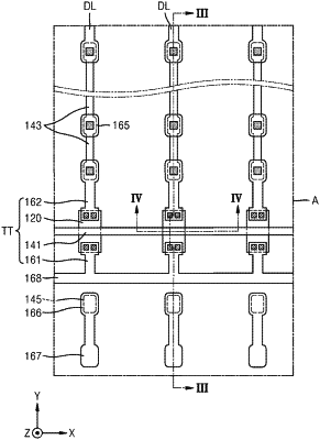
1. A method of determining whether a display manufacturing facility is abnormal, the method comprising:
a first step of obtaining facility information data of facilities used to manufacture a display panel;
a second step of preparing a display module by attaching a printed circuit board and a driving chip to the display panel;
a third step of obtaining preliminary inspection data through an on-off test on the display module;
a fourth step of associating the facility information data with the preliminary inspection data;
establishing a database by repeatedly performing the first step to the fourth step;
obtaining real-time inspection data through an on-off test on a display module to be inspected;
determining, from the real-time inspection data, whether the display module to be inspected is normal; and,
determining a facility causing abnormality of the display module, from the real-time inspection data by using the database in case that the display module to be inspected is determined to be abnormal.
|