| CPC C09K 13/10 (2013.01) [C09K 13/08 (2013.01); H01L 21/30604 (2013.01); H10B 12/05 (2023.02); H10B 12/30 (2023.02)] | 13 Claims |
|
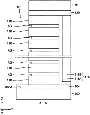
1. A method of manufacturing an integrated circuit device, the method comprising:
forming, on a substrate, a structure in which a plurality of silicon films and a plurality of silicon germanium films are alternately stacked; and
selectively removing the plurality of silicon germanium films from among the plurality of silicon films by using an etchant composition,
wherein the etchant composition includes:
about 5 wt % to about 14 wt % of an oxidant, based on a total weight of the etchant composition;
about 0.01 wt % to about 5 wt % of a fluorine compound, based on the total weight of the etchant composition;
about 0.01 wt % to about 5 wt % of an amine compound, based on the total weight of the etchant composition;
about 0.01 wt % to about 1 wt % of an alcohol compound having a hydrophilic head and a hydrophobic tail, based on the total weight of the etchant composition;
about 60 wt % to about 90 wt % of an organic solvent, based on the total weight of the etchant composition; and
a balance of water.
|