| CPC C03B 11/00 (2013.01) [C03B 23/20 (2013.01); G06F 1/1633 (2013.01); C03B 2215/406 (2013.01); C03B 2215/41 (2013.01)] | 19 Claims |
|
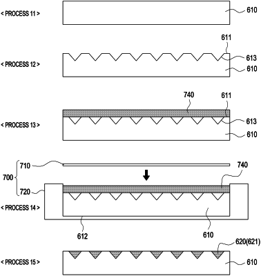
1. A back surface plate configured to form a back surface of an electronic device, the back surface plate comprising:
a first glass part including a first pattern area including a pattern having a predetermined shape on a first surface; and
a second glass part at least portion of which is disposed on the first surface of the first glass part, the second glass part including a first shape complimentary to the first pattern area,
wherein the second glass part has a color different from a color of the first glass part,
wherein a softening point of the second glass part is lower than a softening point of the first glass part.
|