| CPC H10K 59/88 (2023.02) [G01R 31/2884 (2013.01); H10K 50/822 (2023.02); H10K 71/00 (2023.02); H10K 50/828 (2023.02); H10K 59/12 (2023.02); H10K 59/1201 (2023.02)] | 13 Claims |
|
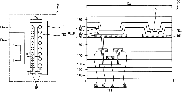
1. A display device comprising:
a substrate including a display area and a test area adjacent to the display area;
a lower electrode disposed in the display area on the substrate;
a light emitting layer disposed on the lower electrode;
a common layer disposed on the light emitting layer;
an upper electrode disposed on the common layer; and
a test element group including:
a plurality of electrode patterns disposed in a same layer as the lower electrode and in the test area on the substrate;
a test common layer disposed in a same layer as the common layer and on the plurality of electrode patterns, wherein a plurality of openings is defined through the test common layer to expose a part of each of the plurality of electrode patterns; and
an electrode layer disposed in a same layer as the upper electrode, on the test common layer, and in contact with the plurality of electrode patterns through the plurality of openings.
|