| CPC H10K 59/1315 (2023.02) [H10K 50/844 (2023.02); H10K 59/122 (2023.02); H10K 59/124 (2023.02); H10K 59/1213 (2023.02); G09G 3/3233 (2013.01); G09G 2300/0809 (2013.01)] | 12 Claims |
|
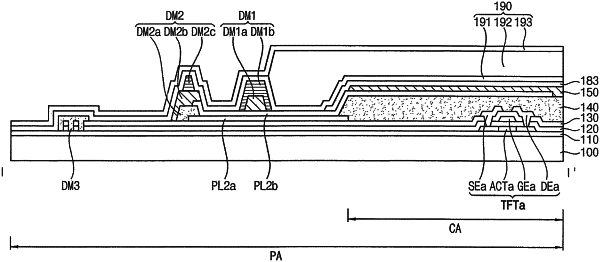
1. A display apparatus, comprising:
a substrate;
a first-layer power supply line disposed on the substrate in a peripheral area which does not display an image, the peripheral area surrounds a display area in which an image is displayed;
a second-layer power supply line disposed only in the peripheral area and disposed on the first-layer power supply line, and contacting the first-layer power supply line; and
a light emitting structure comprising a first electrode, a light emitting layer disposed on the first electrode, and a second electrode disposed on the light emitting layer and electrically connected to the second-layer power supply line,
wherein the first-layer power supply line and the second-layer power supply line supply a power voltage to the second electrode which acts as a cathode of the light emitting structure.
|