| CPC H10K 59/131 (2023.02) [H01L 27/124 (2013.01); H01L 27/1225 (2013.01); H01L 27/1255 (2013.01); H01L 29/7869 (2013.01); H01L 29/78651 (2013.01); H10K 50/80 (2023.02); H10K 50/88 (2023.02); H10K 59/1213 (2023.02); H10K 59/1315 (2023.02)] | 20 Claims |
|
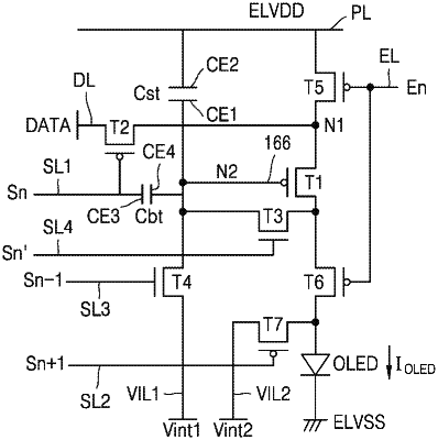
1. A display device comprising:
a first transistor;
a second transistor connected to a data line and the first transistor;
a third transistor connected to a node and the first transistor;
a fourth transistor connected to the node and a first initialization voltage line;
a fifth transistor connected to a power supply voltage line and the first transistor;
a sixth transistor connected to the first transistor and a light emitting device;
a seventh transistor connected to the light emitting device and a second initialization voltage line; and
a first capacitor connected to a driving voltage line and the node,
wherein each of the first to the seventh transistors comprises a semiconductor layer and a gate electrode, the semiconductor layer comprising a source region, a drain region and a channel region overlapped with the gate electrode,
wherein the gate electrode of the first transistor is connected to the node,
wherein each of the semiconductor layer of the third transistor and the semiconductor layer of the fourth transistor comprises oxide semiconductor, and
wherein the power supply voltage line overlaps the channel region of the semiconductor layer of the third transistor and the channel region of the semiconductor layer of the fourth transistor.
|