| CPC H10K 59/131 (2023.02) [G09G 3/3233 (2013.01); G09G 3/3266 (2013.01); H01L 27/124 (2013.01); H01L 27/1248 (2013.01); H01L 27/1255 (2013.01); H10K 59/122 (2023.02); H10K 59/123 (2023.02); H10K 59/124 (2023.02); H10K 59/1213 (2023.02); H10K 59/1216 (2023.02); H10K 59/352 (2023.02); H10K 59/88 (2023.02); G09G 3/3225 (2013.01); G09G 2300/0413 (2013.01); G09G 2300/0426 (2013.01); G09G 2310/0232 (2013.01); G09G 2310/0281 (2013.01); G09G 2320/0223 (2013.01); H10K 59/35 (2023.02)] | 19 Claims |
|
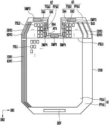
1. A display device, comprising:
a substrate comprising a first display region, and second and third display regions extending from the first display region;
first pixels in the first display region and first lines electrically connected to the first pixels;
second pixels in the second display region and second lines electrically connected to the second pixels;
third pixels in the third display region and third lines electrically connected to the third pixels; and
a first dummy part located between the second pixels and the third pixels,
wherein the first dummy part is electrically connected to a portion of the second lines and a portion of the third lines,
wherein the second display region comprises a first sub-region adjacent to the first display region and a second sub-region adjacent to the first sub-region, and
wherein the third display region comprises a third sub-region adjacent to the first display region and a fourth sub-region adjacent to the third sub-region.
|