| CPC H10K 59/131 (2023.02) [G06F 3/0412 (2013.01); G06F 3/04164 (2019.05); H10K 50/844 (2023.02); H10K 59/124 (2023.02); H10K 59/40 (2023.02); G06F 3/0446 (2019.05)] | 17 Claims |

|
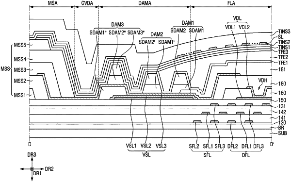
1. A display device comprising:
a substrate;
a first active layer disposed on the substrate and including a channel region;
a first gate insulating film disposed on the first active layer;
a first gate electrode disposed on the first gate insulating film and overlapping the channel region of the first active layer;
a first interlayer insulating film disposed on the first gate electrode;
a capacitor electrode disposed on the first interlayer insulating film and overlapping the first gate electrode;
a second interlayer insulating film disposed on the capacitor electrode;
a first sub power supply line and a third sub power supply line disposed on the second interlayer insulating film;
a second sub power supply line disposed on the first sub power supply line;
a fourth sub power supply line disposed on the third sub power supply line; and
a first planarization film disposed between the third sub power supply line and the fourth sub power supply line,
wherein at least one of the first sub power supply line and the second sub power supply line overlaps at least one of the third sub power supply line and the fourth sub power supply line.
|