| CPC H10K 59/131 (2023.02) [G09G 3/3233 (2013.01); H01L 27/124 (2013.01); G09G 2300/0426 (2013.01); G09G 2310/0264 (2013.01)] | 20 Claims |

|
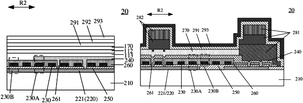
1. A display substrate, having a display region and a peripheral region at least partially surrounding the display region, and comprising: a base substrate, a semiconductor pattern, at least one wire, and a conductive pattern,
wherein the display region has an opening, and the peripheral region comprises an opening peripheral region at least partially in the opening;
the semiconductor pattern and the conductive pattern are on the base substrate and in the opening peripheral region;
the at least one wire is in the display region and the opening peripheral region, and is configured to transmit an electrical signal for the display region;
each of the at least one wire comprises a first portion and a second portion; and
in a direction perpendicular to the base substrate, the first portion is spaced apart and insulated from the semiconductor pattern and the conductive pattern, to provide at least one first compensation unit with a first capacitor structure, and the second portion is spaced apart and insulated from one of the semiconductor pattern and the conductive pattern, to provide at least one second compensation unit with a second capacitor structure.
|