| CPC H10K 59/131 (2023.02) [G09G 3/3258 (2013.01); G09G 2300/0426 (2013.01); G09G 2300/0842 (2013.01)] | 18 Claims |
|
1. An array substrate, comprising a pixel driving circuit;
wherein the pixel driving circuit comprises a driving transistor; a first transistor; a second transistor; a third transistor, a fourth transistor, a fifth transistor, a sixth transistor, and a storage capacitor;
wherein a gate electrode of the driving transistor is electrically connected to a first electrode of the third transistor, a second electrode of the first transistor, and a first capacitor electrode of the storage capacitor;
a first electrode of the driving transistor is electrically connected to a second electrode of the second transistor and a second electrode of the fourth transistor;
a second electrode of the driving transistor is electrically connected to a second electrode of the third transistor and a first electrode of the fifth transistor;
a second electrode of the fifth transistor is electrically connected to a second electrode of the sixth transistor; and
a first electrode of the fourth transistor is electrically connected to a second capacitor electrode of the storage capacitor;
wherein the array substrate comprises:
a base substrate;
a semiconductor material layer on the base substrate;
a gate insulating layer on a side of the semiconductor material layer away from the base substrate;
a plurality of gate lines respectively extending along a first direction and the first capacitor electrode of the storage capacitor on a side of the gate insulating layer away from the base substrate;
an insulating layer on a side of the plurality of gate lines away from the base substrate;
an interference preventing block and the second capacitor electrode on a side of the insulating layer away from the base substrate;
an inter-layer dielectric layer on a side of the interference preventing block and the second capacitor electrode away from the base substrate; and
a plurality of data lines respectively extending along a second direction, a plurality of voltage supply lines respectively extending along the second direction, a node connecting line on a side of the inter-layer dielectric layer away from the base substrate;
wherein the second capacitor electrode is electrically connected to a respective one of the plurality of voltage supply lines;
the node connecting line is connected to the first capacitor electrode through a first through hole, and connected to the first electrode of the third transistor through a second through hole; and
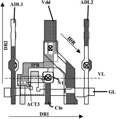
the respective one of the plurality of voltage supply lines is connected to the interference preventing block through a third through hole, the interference preventing block comprising a first arm and a second arm;
wherein in a plan view of a virtual line parallel to the first direction, the virtual line intersects with the node connecting line at a position of the second through hole; and wherein, along the first direction of the plan view of the virtual line, a first adjacent data line, the first arm, the node connecting line at the position of the second through hole, the second arm, and a second adjacent data line are sequentially arranged.
|