| CPC H10K 59/131 (2023.02) [H10K 59/126 (2023.02); H10K 59/1213 (2023.02); H10K 59/1216 (2023.02); H10K 71/00 (2023.02); H10K 59/1201 (2023.02)] | 20 Claims |
|
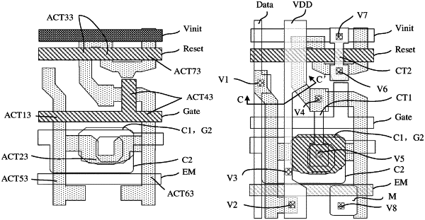
1. A display panel, comprising a substrate and a plurality of sub-pixels located on the substrate, at least one sub-pixel of the plurality of sub-pixels comprising:
a light emitting element comprising an anode and a cathode;
a first transistor comprising a first active layer and a first gate which is connected to a scan line, the first active layer comprising a first electrode region, a second electrode region, and a first channel region located between the first electrode region and the second electrode region, wherein the first electrode region is connected to a data line, and the second electrode region is connected to a power line;
a capacitor comprising a first electrode plate and a second electrode plate connected to the power line;
a second transistor comprising a second active layer and a second gate which is connected to the first electrode plate, the second active layer comprising a third electrode region, a fourth electrode region, and a second channel region located between the third electrode region and the fourth electrode region, wherein the third electrode region is connected to the second electrode region, and the fourth electrode region is connected to the anode; and
a third transistor comprising a third active layer and a third gate which is connected to a reset line, the third active layer comprising a fifth electrode region, a sixth electrode region, and a third channel region located between the fifth electrode region and the sixth electrode region, wherein the fifth electrode region is connected to the first electrode plate, and the sixth electrode region is connected to an initialization voltage line,
wherein an orthographic projection of the power line on the substrate is a first projection, an orthographic projection of the reset line on the substrate is a second projection, an orthographic projection of the third channel region on the substrate is a third projection, and an orthographic projection of the data line on the substrate is a fourth projection, and
wherein an region of the first projection overlapping with the second projection and the third projection is a first region, and regions of the first projection overlapping with the second projection and not overlapping with the third projection comprise a second region and a third region that are adjacent to the first region, wherein the second region is located on one side of the first region proximate to the fourth projection, and the third region is located on one side of the first region away from the fourth projection, and an area of the second region is not smaller than an area of the third region.
|