| CPC H10K 59/131 (2023.02) [H10K 71/00 (2023.02); H10K 59/1201 (2023.02)] | 20 Claims |
|
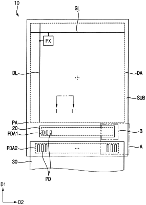
1. A display apparatus comprising:
a substrate including a display area and a peripheral area disposed outside the display area;
a transistor disposed in the display area on the substrate;
a first pad part disposed in the peripheral area on the substrate;
a second pad part disposed in the peripheral area on the substrate and spaced apart from the first pad part;
a first pad disposed in the second pad part;
a second pad disposed in the second pad part and spaced apart from the first pad; and
a passivation layer including a plurality of grooves defined between the first pad and the second pad and a protrusion disposed between two adjacent grooves among the grooves.
|