| CPC H10K 59/131 (2023.02) [G09G 3/3225 (2013.01); H10K 50/844 (2023.02); H10K 59/122 (2023.02); H10K 71/00 (2023.02); H10K 59/1201 (2023.02)] | 15 Claims |
|
1. A display panel comprising:
a display unit including an active area displaying an image; and
a driving unit connected to the display unit,
wherein the display unit comprises:
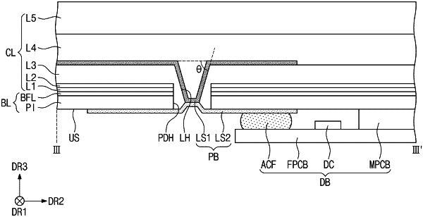
a base layer including a front surface and a rear surface opposing each other;
a circuit element layer disposed on the front surface of the base layer and including a plurality of insulating layers and a transistor having a plurality of electrodes disposed between the insulating layers;
a display element layer disposed on the circuit element layer and including a light emitting element connected to the transistor; and
a pad unit including a connection line branched from an electrode of the plurality of electrodes and a pad line connected to the driving unit,
the display unit defines a pad hole passing through the base layer and at least one insulating layer of the plurality of insulating layers,
a third insulating layer of the plurality of insulating layers covers a side surface of the at least one insulating layer defining the pad hole, is different from the at least one insulating layer, and defines an insulating hole passing through the third insulating layer,
the third insulating layer is in direct contact with an upper surface and the side surface of the at least one insulating layer and a side surface of the base layer defining the pad hole, and
the connection line and the pad line are in contact with each other inside the insulating hole.
|