| CPC H10K 59/128 (2023.02) [B06B 1/0688 (2013.01); H10K 59/00 (2023.02); H10K 71/00 (2023.02); H10K 59/1201 (2023.02)] | 20 Claims |
|
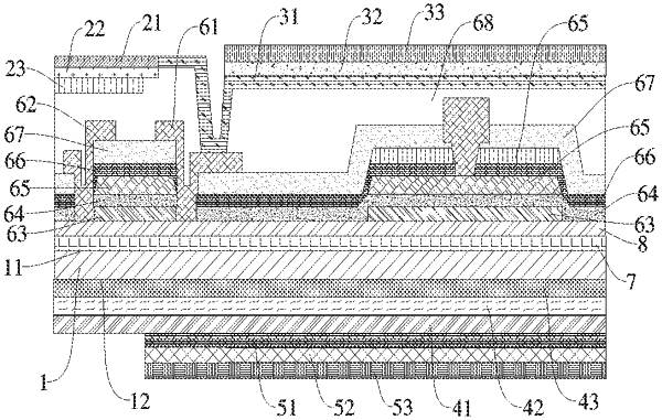
1. A display substrate, comprising:
a base substrate having a first side and a second side opposite to each other;
a transmitter arranged on the first side of the base substrate, and configured to convert a first display electrical signal into a conduction signal;
a first light-emitting element arranged on a side of the transmitter away from the base substrate, wherein the first light-emitting element emits light under a driving action of the first display electrical signal;
a receiver arranged on the second side of the base substrate, and configured to receive the conduction signal and convert the conduction signal into a second display electrical signal; and
a second light-emitting element arranged on a side of the receiver away from the base substrate, wherein the second light-emitting element emits light under a driving action of the second display electrical signal.
|