US 11,910,657 B2
OLED panel with inorganic pixel encapsulating barrier
Ji-young Choung, Hwaseong-si (KR); Dieter Haas, San Jose, CA (US); Yu Hsin Lin, Zhubei (TW); Jungmin Lee, Santa Clara, CA (US); Seong Ho Yoo, San Ramon, CA (US); and Si Kyoung Kim, Gwangju-si (KR)
Assigned to Applied Materials, Inc., Santa Clara, CA (US)
Filed by Applied Materials, Inc., Santa Clara, CA (US)
Filed on Jun. 30, 2023, as Appl. No. 18/346,059.
Application 18/346,059 is a continuation of application No. 18/314,915, filed on May 10, 2023.
Application 18/314,915 is a continuation of application No. 18/049,868, filed on Oct. 26, 2022, granted, now 11,690,255, issued on Jun. 27, 2023.
Application 18/049,868 is a continuation of application No. 18/049,825, filed on Oct. 26, 2022, granted, now 11,690,254, issued on Jun. 27, 2023.
Application 18/049,825 is a continuation of application No. 17/498,482, filed on Oct. 11, 2021, granted, now 11,476,313, issued on Oct. 18, 2022.
Application 17/498,482 is a continuation of application No. 17/193,321, filed on Mar. 5, 2021, abandoned.
Claims priority of provisional application 63/084,445, filed on Sep. 28, 2020.
Claims priority of provisional application 63/075,028, filed on Sep. 4, 2020.
Claims priority of provisional application 63/075,025, filed on Sep. 4, 2020.
Prior Publication US 2023/0345771 A1, Oct. 26, 2023
This patent is subject to a terminal disclaimer.
Int. Cl. H10K 59/122 (2023.01); H10K 50/844 (2023.01); H10K 50/84 (2023.01); H10K 71/00 (2023.01); H10K 59/12 (2023.01)
CPC H10K 59/122 (2023.02) [H10K 50/84 (2023.02); H10K 50/844 (2023.02); H10K 71/00 (2023.02); H10K 59/1201 (2023.02)] 23 Claims
OG exemplary drawing
 
1. A device, comprising:
a substrate;
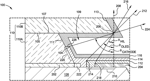
inorganic overhang structures, the inorganic overhang structures having an upper portion having a bottom surface wider than a top surface of a lower portion; and
a plurality of sub-pixels, each sub-pixel comprising:
an anode;
an organic light-emitting diode (OLED) material disposed over the anode;
a cathode disposed over the OLED material, extending under the inorganic overhang structures adjacent to each sub-pixel, the cathode directly contacts a layer of a conductive material disposed under the lower portion; and
an encapsulation layer disposed over the cathode, wherein the encapsulation layer extends under at least a portion of the inorganic overhang structures along a sidewall of the lower portion, and contacts the bottom surface of the upper portion of the inorganic overhang structures.