| CPC H10K 59/122 (2023.02) [G09G 3/3291 (2013.01); H10K 59/35 (2023.02); H10K 71/00 (2023.02); H10K 71/621 (2023.02); G09G 2320/0214 (2013.01)] | 23 Claims |
|
1. A display comprising:
a substrate;
an array of pixels that includes first and second organic light-emitting diode pixels, wherein the first organic light-emitting diode pixel includes a first patterned electrode on the substrate and wherein the second organic light-emitting diode pixel includes a second patterned electrode on the substrate;
a pixel definition layer on the substrate that is interposed between the first and second patterned electrodes;
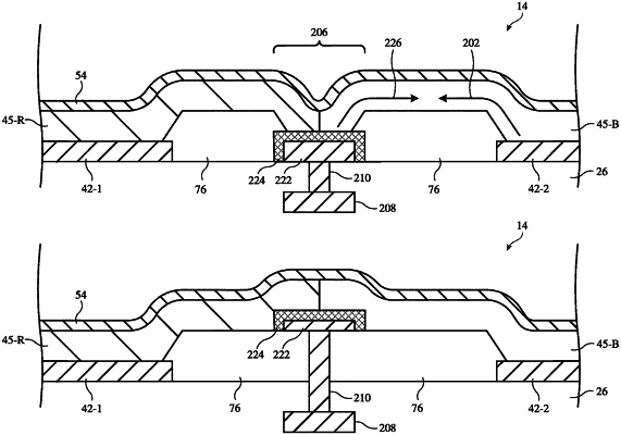
a conductive layer formed over the substrate that has a first portion that forms part of the first organic light-emitting diode pixel and a second portion that forms part of the second organic light-emitting diode pixel;
a conductive gate that is formed between the first and second patterned electrodes, wherein the conductive gate is coupled to a variable gate voltage and is configured to generate a current that mitigates leakage current through the conductive layer;
a metal layer in the substrate; and
a via that electrically connects the conductive gate to the metal layer.
|