| CPC H10K 59/1213 (2023.02) [H10K 59/123 (2023.02); H10K 59/124 (2023.02)] | 20 Claims |
|
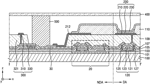
1. A display apparatus comprising:
a lower substrate comprising a display area and a non-display area;
a thin film transistor on the lower substrate in a first direction at the display area;
a display element at the display area and electrically connected to the thin film transistor;
a discharge element at the non-display area; and
a driving circuit configured to generate at least one of a scan signal or an emission control signal, the driving circuit being located at the non-display area between the discharge element and the thin film transistor, and spaced from the discharge element in a plan view,
wherein the discharge element comprises at least one electrode layer, at least one discharge layer on the at least one electrode layer and spaced entirely apart from the display element and the driving circuit in a plan view, and at least one first insulating layer on and overlapping with the at least one electrode layer in the first direction between the at least one electrode layer and the at least one discharge layer, and
wherein a distance from an upper surface of the lower substrate to an upper surface of the at least one discharge layer is greater than or equal to a distance from the upper surface of the lower substrate to an upper surface of a top layer of the thin film transistor.
|