| CPC H10K 50/858 (2023.02) [G02B 30/27 (2020.01); H10K 50/865 (2023.02)] | 22 Claims |
|
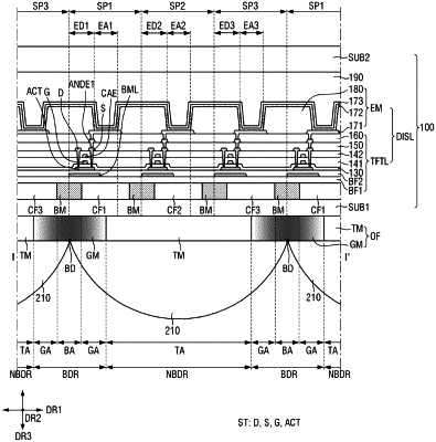
1. A display device comprising:
a display panel;
a lens array disposed on a first surface of the display panel and including a plurality of lenses; and
an optical filter disposed on the first surface of the display panel,
wherein the optical filter includes a plurality of first portions and a plurality of second portions which are alternately arranged in a first direction parallel to the first surface of the display panel,
wherein each of the plurality of first portions has a first transmittance value, and
wherein each of the plurality of second portions has a symmetric light transmittance distribution in which a transmittance value increases from the center having a second transmittance value to each of opposite ends having a third transmittance value.
|