US 11,910,629 B2
Light emitting device, method of manufacturing the same, and display device
Chan Su Kim, Seoul (KR); Kun Su Park, Seongnam-si (KR); Tae Ho Kim, Seongnam-si (KR); Eun Joo Jang, Suwon-si (KR); and Dae Young Chung, Suwon-si (KR)
Assigned to SAMSUNG ELECTRONICS CO., LTD., Gyeonggi-Do (KR)
Filed by SAMSUNG ELECTRONICS CO., LTD., Suwon-si (KR)
Filed on Dec. 7, 2022, as Appl. No. 18/076,495.
Application 18/076,495 is a continuation of application No. 17/008,779, filed on Sep. 1, 2020, granted, now 11,532,800.
Claims priority of application No. 10-2019-0116948 (KR), filed on Sep. 23, 2019.
Prior Publication US 2023/0118092 A1, Apr. 20, 2023
This patent is subject to a terminal disclaimer.
Int. Cl. H01L 51/52 (2006.01); H01L 27/32 (2006.01); H10K 50/115 (2023.01); H10K 50/15 (2023.01); H10K 50/155 (2023.01); H10K 71/00 (2023.01); H10K 71/13 (2023.01); H10K 102/00 (2023.01)
CPC H10K 50/115 (2023.02) [H10K 50/15 (2023.02); H10K 50/155 (2023.02); H10K 50/156 (2023.02); H10K 71/00 (2023.02); H10K 71/135 (2023.02); H10K 2102/331 (2023.02)] 15 Claims
OG exemplary drawing
 
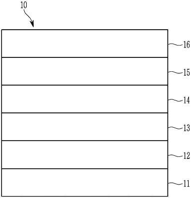
1. A light emitting device comprising
a first electrode,
a second electrode,
a quantum dot layer disposed between the first electrode and the second electrode, and
a first auxiliary layer disposed between the quantum dot layer and the first electrode,
wherein the first auxiliary layer comprises nickel oxide nanoparticles having an average particle diameter of less than or equal to about 10 nanometers, and
wherein about 90% or greater of a total number of the nickel oxide nanoparticles in the first auxiliary layer have a particle size within ± about 30% of the average particle diameter of the nickel oxide nanoparticles.