| CPC H10B 61/22 (2023.02) [H10N 50/01 (2023.02); H10N 50/80 (2023.02)] | 20 Claims |
|
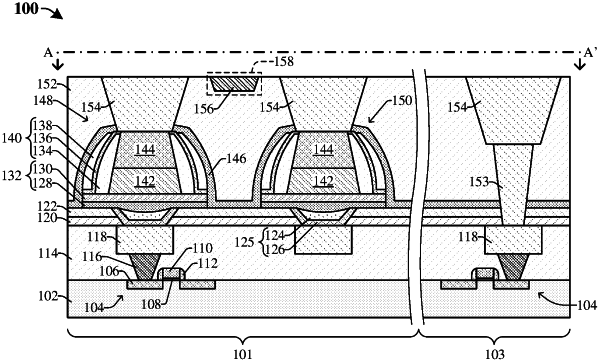
1. A method for forming a memory device, comprising:
forming a first memory cell and a second memory cell over a substrate;
forming a sidewall spacer layer around the first and second memory cells;
forming a first dielectric layer over and around the first and second memory cells, wherein the first dielectric layer comprises sidewalls defining an opening spaced laterally between the first and second memory cells;
forming a second dielectric layer over the first dielectric layer, wherein the second dielectric layer is disposed in the opening;
performing a planarization process on the first and second dielectric layers, wherein at least a portion of the second dielectric layer is in the opening after the planarization process; and
performing an etching process on the first dielectric layer to form a plurality of upper openings over the first and second memory cells, wherein during the etching process the first dielectric layer is etched more quickly than the sidewall spacer layer.
|