| CPC H10B 51/30 (2023.02) [H01L 29/66969 (2013.01); H01L 29/7869 (2013.01); H01L 29/78696 (2013.01); H10B 51/20 (2023.02)] | 20 Claims |
|
1. A method of forming a ferroelectric memory device, comprising:
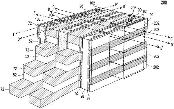
forming a multi-layer stack and comprising a plurality of dielectric layers and a plurality of conductive layers stacked alternately over a substrate, wherein sidewalls of the plurality of dielectric layers and the plurality of conductive layers define a trench penetrating therethrough;
selectively forming a plurality of ferroelectric portions discretely on the sidewalls of the plurality of conductive layers;
after forming the plurality of ferroelectric portions then forming a channel layer on the plurality of ferroelectric portions and the sidewalls of the plurality of dielectric layers; and
forming a conductive pillar along sidewalls of the channel layer.
|