US 11,910,616 B2
Three-dimensional memory device and method
Meng-Han Lin, Hsinchu (TW); Han-Jong Chia, Hsinchu (TW); Sheng-Chen Wang, Hsinchu (TW); Feng-Cheng Yang, Zhudong Township (TW); Yu-Ming Lin, Hsinchu (TW); and Chung-Te Lin, Tainan (TW)
Assigned to TAIWAN SEMICONDUCTOR MANUFACTURING CO., LTD., Hsinchu (TW)
Filed by Taiwan Semiconductor Manufacturing Co., Ltd., Hsinchu (TW)
Filed on Aug. 9, 2022, as Appl. No. 17/818,562.
Application 17/818,562 is a division of application No. 17/140,888, filed on Jan. 4, 2021, granted, now 11,527,553.
Claims priority of provisional application 63/058,619, filed on Jul. 30, 2020.
Prior Publication US 2022/0384347 A1, Dec. 1, 2022
Int. Cl. H10B 51/20 (2023.01); H01L 29/417 (2006.01); H01L 23/535 (2006.01); H10B 51/00 (2023.01); H10B 51/10 (2023.01); H10B 51/30 (2023.01)
CPC H10B 51/20 (2023.02) [H01L 23/535 (2013.01); H01L 29/41741 (2013.01); H01L 29/41775 (2013.01); H10B 51/00 (2023.02); H10B 51/10 (2023.02); H10B 51/30 (2023.02)] 20 Claims
OG exemplary drawing
 
1. A device comprising:
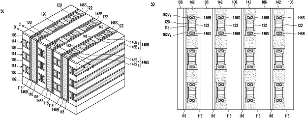
a word line extending in a first direction;
a data storage layer on a sidewall of the word line;
a channel layer on a sidewall of the data storage layer;
a back gate isolator on a sidewall of the channel layer; and
a bit line having a first main region and a first extension region, the first main region contacting the channel layer, the first extension region separated from the channel layer by the back gate isolator, the bit line extending in a second direction, the second direction perpendicular to the first direction.