| CPC H10B 51/20 (2023.02) [H10B 51/10 (2023.02)] | 20 Claims |
|
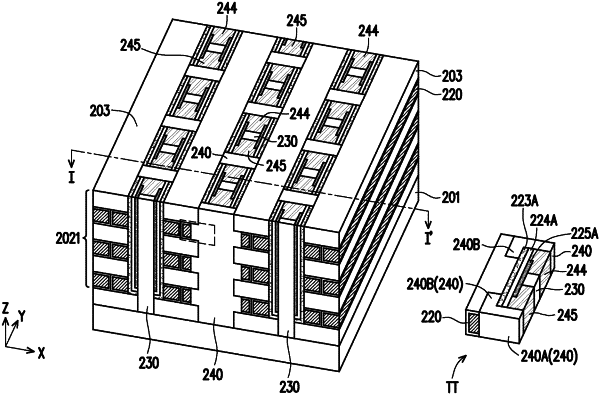
1. A memory device, comprising:
a multilayered stack disposed over a dielectric structure, the multilayered stack comprising first conductive layers and first dielectric layers stacked in alternation;
a second dielectric layer, disposed over the dielectric structure and penetrating through the first conductive layers and the first dielectric layers;
a first conductive line and a second conductive line disposed at opposite sides of the second dielectric layer;
a pair of dielectric blocks respectively disposed alongside the first conductive line and the second conductive line;
a memory layer, disposed between the pair of dielectric blocks and penetrating through the first conductive layers and the first dielectric layers; and
a channel material layer, disposed between the pair of dielectric blocks, extending vertically along the memory layer, and disposed between the first and second conductive lines and the memory layer,
wherein each of the pair of dielectric blocks has an extended portion located between the memory layer and one of the first conductive layers, and a material of the pair of dielectric blocks has a dielectric constant lower than that of a material of the memory layer.
|