| CPC H10B 43/40 (2023.02) [H01L 21/0217 (2013.01); H01L 21/02164 (2013.01); H01L 21/02532 (2013.01); H01L 21/02592 (2013.01); H01L 21/2251 (2013.01); H01L 21/31111 (2013.01); H01L 21/32053 (2013.01); H01L 23/528 (2013.01); H01L 29/458 (2013.01); H01L 29/665 (2013.01); H01L 29/66742 (2013.01); H01L 29/78642 (2013.01); H10B 43/10 (2023.02); H10B 43/27 (2023.02)] | 8 Claims |

|
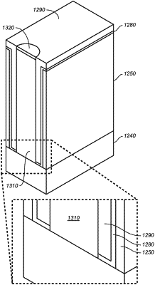
1. A process for forming a transistor above a planar surface of a substrate, comprising:
Providing first and second conductive layers comprising each a material that is suitable for the first and the second conductive layers to form a drain region and a source region of the transistor, respectively, the first and second conductive layers being isolated from each other by an isolation layer;
providing an active layer in contact with both the first and second conductive layers, wherein the active layer comprises a material suitable for forming a channel region of the transistor and wherein a portion of the active layer is provided above either the first conductive layer or the second conductive layer;
providing a gate dielectric layer over the active layer;
providing a third conductive layer over gate dielectric layer;
etching the active layer, the gate dielectric layer and the third conductive layer to form a line structure around the second conductive layer, the isolation layer and the first conductive layer;
providing a passivation layer to enclose the third conductive layer, the gate dielectric layer, the first and the second conductive layers, the active layer, and the isolation layer;
etching the passivation layer to provide a via to expose a portion of the second conductive layer or a portion of the first conductive layer; and
providing a metallic layer on the exposed portion of second conductive layer or the exposed portion of the first conductive layer.
|