| CPC H10B 43/27 (2023.02) [H01L 23/5283 (2013.01); H10B 41/10 (2023.02); H10B 41/27 (2023.02); H10B 41/35 (2023.02); H10B 41/40 (2023.02); H10B 43/10 (2023.02); H10B 43/35 (2023.02); H10B 43/40 (2023.02)] | 20 Claims |
|
1. A semiconductor device, comprising:
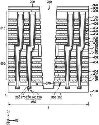
a gate electrode structure on a substrate, the gate electrode structure including gate electrodes spaced apart from each other in a first direction perpendicular to an upper surface of the substrate and stacked in a staircase shape;
a channel extending through the gate electrode structure, the channel including:
a first portion extending in the first direction on the substrate; and
a second portion extending in the first direction on and contacting the first portion, a lower surface of the second portion having a width less than a width of an upper surface of the first portion; and
an etch stop layer on a sidewall of the gate electrode structure and contacting at least one gate electrode of the gate electrodes, the etch stop layer overlapping an upper portion of the first portion of the channel in a horizontal direction parallel to the upper surface of the substrate,
wherein the at least one gate electrode contacting the etch stop layer is a dummy gate electrode including an insulating material.
|