| CPC H10B 43/27 (2023.02) [H01L 23/5226 (2013.01); H10B 41/27 (2023.02)] | 23 Claims |
|
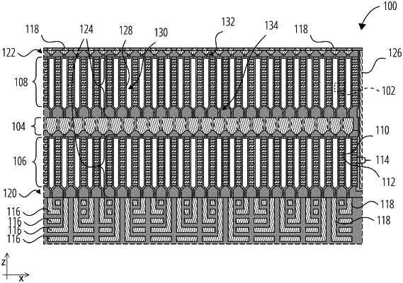
1. A microelectronic device, comprising:
a pair of stack structures, the pair comprising:
a lower stack structure; and
an upper stack structure overlying the lower stack structure,
the lower stack structure and the upper stack structure each comprising a vertically alternating sequence of insulative structures and conductive structures arranged in tiers;
a source region vertically interposed between the lower stack structure and the upper stack structure, the source region comprising at least one conductive material comprising, along a lower surface thereof, an array of V-shaped extensions;
a first array of pillars extending, through the upper stack structure, from proximate the source region toward a first drain region above the upper stack structure; and
a second array of pillars extending, through the lower stack structure, from proximate the source region toward a second drain region below the lower stack structure.
|