| CPC H10B 41/27 (2023.02) [H10B 41/35 (2023.02); H10B 41/41 (2023.02); H10B 43/27 (2023.02); H10B 43/35 (2023.02); H10B 43/40 (2023.02)] | 14 Claims |

|
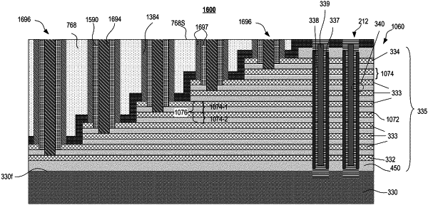
1. A memory device, comprising:
a film stack, comprising a dielectric layer and a conductive layer alternatingly stacked in a first direction;
a staircase structure disposed in the film stack and comprising a staircase step, wherein the staircase step comprises two or more alternatingly stacked dielectric layers and conductive layers;
a barrier layer and a first insulating layer disposed on the staircase structure; and
a coaxial contact structure disposed on the staircase step and extending through the first insulating layer and the barrier layer in the first direction, wherein:
the coaxial contact structure comprises a conductive ring, an insulating ring and a conductive core, wherein the insulating ring is disposed between the conductive ring and the conductive core;
a bottom surface of the conductive core contacts a lowermost conductive layer of the staircase step;
a bottom surface of the conductive ring contacts an upper conductive layer stacked above the lowermost conductive layer; and
a bottom surface of the insulating ring contacts a corresponding dielectric layer disposed between the lowermost conductive layer and the upper conductive layer of the staircase step.
|