| CPC H10B 12/37 (2023.02) [H10B 12/0387 (2023.02); H10B 12/482 (2023.02); H10B 12/50 (2023.02)] | 20 Claims |
|
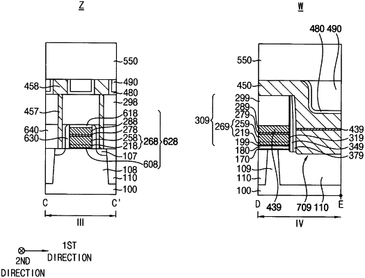
1. A semiconductor device comprising:
a substrate including:
a chip region; and
a scribe lane region surrounding the chip region;
a bit line structure on the chip region of the substrate, the bit line structure having a stacked structure including multiple layers stacked on each other;
a first spacer structure on a sidewall of the bit line structure;
a key structure on the scribe lane region of the substrate, the key structure having the same stacked structure as the bit line structure;
a second spacer structure on a sidewall of the key structure;
a filling pattern on the scribe lane region of the substrate, the filling pattern being adjacent to the second spacer structure and including a conductive material; and
a first conductive structure on the filling pattern, the key structure and the second spacer structure.
|