| CPC H05K 3/181 (2013.01) [H05K 1/09 (2013.01); H05K 1/117 (2013.01); H05K 3/027 (2013.01); H05K 3/188 (2013.01); H05K 3/403 (2013.01); H05K 5/0026 (2013.01); H05K 2203/0502 (2013.01)] | 11 Claims |
|
1. An electronic device, comprising:
a first circuit board;
a second circuit board;
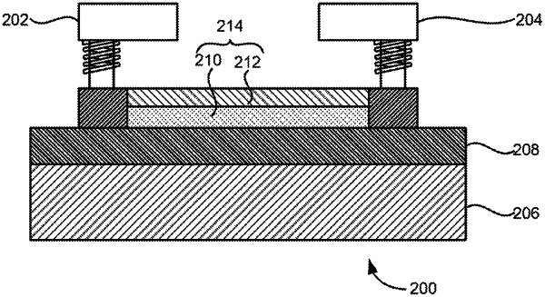
a housing to house the first circuit board and the second circuit board;
an insulating adhesive layer formed on a surface of the housing;
a patterned electroconductive layer formed on the insulating adhesive layer to electrically connect the first circuit board and the second circuit board, wherein the patterned electroconductive layer comprises:
a patterned electroless plating layer formed on the insulating adhesive layer; and
a patterned electrolytic plating layer formed on the patterned electroless plating layer;
a first contact pad formed on the insulating adhesive layer and connected to a first end of the patterned electroconductive layer;
a second contact pad formed on the insulating adhesive layer and connected to a second end of the patterned electroconductive layer, wherein the first contact pad is electrically connected to the second contact pad using the patterned electroconductive layer;
a first surface contact connector having a first end connected to the first circuit board via a first spring and a second end physically engaged with the first contact pad; and
a second surface contact connector having a first end connected to the second circuit board via a second spring and a second end physically engaged with the second contact pad.
|