| CPC H05K 3/0094 (2013.01) [H05K 1/111 (2013.01); H05K 1/141 (2013.01); H05K 1/144 (2013.01); H05K 3/429 (2013.01); H05K 1/181 (2013.01); H05K 2201/09036 (2013.01); H05K 2201/09909 (2013.01)] | 6 Claims |
|
1. A printed circuit board stack structure, comprising:
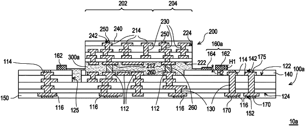
a first printed circuit board having a first surface and a second surface opposite to each other and at least one overflow groove extending from the first surface toward the second surface, and comprising a plurality of first pads located on the first surface and a retaining wall surrounding the first pads;
a second printed circuit board disposed on the first printed circuit board, and comprising a plurality of second pads and a plurality of conductive pillars located on some of the second pads, wherein the conductive pillars are respectively connected to some of the first pads so that the second printed circuit board is electrically connected to the first printed circuit board; and
a filling glue layer filled between the first printed circuit board and the second printed circuit board and covering the first pads, the second pads, and the conductive pillars, wherein the retaining wall blocks the filling glue layer so that a portion of the filling glue layer is accommodated in the at least one overflow groove;
wherein a size of the first printed circuit board is larger than a size of the second printed circuit board, the second printed circuit board has a first density circuit area and a second density circuit area, and a wiring density in the first density circuit area is greater than a wiring density in the second density circuit area; and
wherein the at least one overflow groove is one overflow groove, the retaining wall comprises a first retaining wall and a second retaining wall, a first height of the first retaining wall is greater than a second height of the second retaining wall, the first retaining wall surrounds the first pads, the second retaining wall, and the overflow groove, the first density circuit area is relatively close to the overflow groove and the second density circuit area is relatively close to the second retaining wall, and the overflow groove, the first retaining wall, and the second retaining wall restrict the filling glue layer so that the filling glue layer is located inside the first retaining wall.
|