| CPC H05K 1/0393 (2013.01) [G06F 3/044 (2013.01); G06F 3/0412 (2013.01); H05K 1/0298 (2013.01); H05K 1/118 (2013.01); B32B 2457/208 (2013.01); H05K 2201/0108 (2013.01); H05K 2201/0145 (2013.01)] | 22 Claims |

|
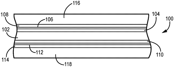
1. A double sided conductive structure comprising:
a transparent polymer substrate comprising a polymer and having a first surface and a second surface, wherein the polymer substrate has an average thickness of no more than about 27 microns and the polymer in a configuration of the transparent polymer substrate has a transmittance from 400 nm to 750 nm of at least about 88% and over the UV spectrum from 330 nm to 375 nm of no more than about 15%;
a first sparse metal conductive layer supported on the first surface of the transparent polymer substrate;
a second sparse metal conductive layer supported on the second surface of the transparent polymer substrate; and
first and second polymer overcoats over the first and second sparse metal conductive layers, respectively, wherein each of the first and second polymer overcoats has an average thickness from about 10 nm to about 200 nm;
wherein each surface of the double sided conductive structure has a sheet resistance of no more than about 120 Ohms/sq.
|