| CPC H03K 5/01 (2013.01) [G06F 1/06 (2013.01); H03K 3/037 (2013.01); H03K 19/20 (2013.01); H03K 2005/00013 (2013.01)] | 20 Claims |
|
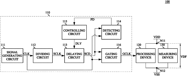
1. A system, comprising:
a measuring device configured to measure a voltage difference between a first node and a second node;
a processing device coupled between the first node and the second node; and
a signal generating device configured to provide a first clock signal to the processing device to adjust the voltage difference, configured to generate the first clock signal according to a first enable signal and a second clock signal, and configured to align an edge of the first enable signal with an edge of the second clock signal.
|